At AboutMechanics, we're committed to delivering accurate, trustworthy information. Our expert-authored content is rigorously fact-checked and sourced from credible authorities. Discover how we uphold the highest standards in providing you with reliable knowledge.
What is an Ion Implant?
Ion implantation has applications in several different industries, most notably in the making of semiconductors. An ion implant is an ion of a particular element, placed in its surrounding material for the purpose of changing the electrical or surface properties of the material. Some common elements that can be used in ion implantation are phosphorous, arsenic, boron, and nitrogen.
The science of ion implantation has been known since the 1950s, but was not in wide use until the 1970s. A machine called a mass separator is used to implant ions in their destination material, which is called the "substrate" for scientific purposes. In a typical setup, ions are produced at a source point and then accelerated toward a separation magnet, which effectively concentrates and aims the ions toward their destination. The ions consist of atoms or molecules with a number of electrons which is higher or lower than usual, making them more chemically active.
Upon reaching the substrate, these ions collide with atoms and molecules before coming to a stop. Such collisions may involve the nucleus of the atom or an electron. The damage caused by these collisions changes the electrical properties of the substrate. In many cases, the ion implant affects the substrate’s ability to conduct electricity.
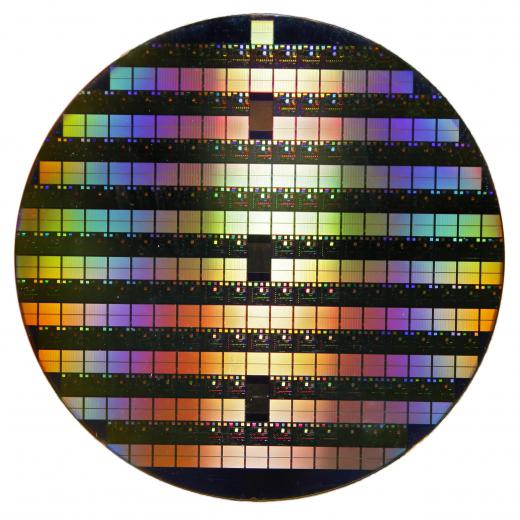
A technique called doping is the primary purpose for using an ion implant. This is commonly done in the production of integrated circuits, and indeed, modern circuits like those in computers could not be made with out ion implantation. Doping is basically another name for ion implantation that applies specifically to circuit manufacturing.
Doping requires that the ions be produced from a very pure gas, which can sometimes be hazardous. Because of this, there are many safety protocols governing the process of doping silicon wafers. Particles of the gas are accelerated and steered toward the silicon substrate in an automated mass separator. Automation reduces safety issues, and several circuits per minute can be doped in this way.
Ion implantation can also be used in making steel tools. The purpose of an ion implant in this case is to change the surface properties of the steel, and make it more resistant to cracks. This change is caused by a slight compression of the surface due to implantation. The chemical change brought about by the ion implant can also guard against corrosion. This same technique is used to engineer prosthetic devices such as artificial joints, giving them similar properties.
AS FEATURED ON:
AS FEATURED ON:

-
![There are many safety protocols governing the process of doping silicon wafers.]() By: Vasily SmirnovThere are many safety protocols governing the process of doping silicon wafers.
By: Vasily SmirnovThere are many safety protocols governing the process of doping silicon wafers.

Discuss this Article
Post your comments