At AboutMechanics, we're committed to delivering accurate, trustworthy information. Our expert-authored content is rigorously fact-checked and sourced from credible authorities. Discover how we uphold the highest standards in providing you with reliable knowledge.
What is a Plasma Etcher?
A plasma etcher is a device that uses plasma to create the circuit pathways needed by semiconductor integrated circuits. The plasma etcher does this by emitting a precisely aimed jet of plasma onto a silicon wafer. When the plasma and the wafer come into contact with one another, a chemical reaction occurs at the surface of the wafer. This reaction either deposits silicon dioxide on the wafer, creating electrical pathways, or removes already present silicon dioxide, leaving only the electrical pathways.
The plasma that a plasma etcher uses is created by super-heating a gas containing either oxygen or fluorine, depending on whether it is to remove or deposit silicon dioxide. This is accomplished by first establishing a vacuum in the etcher and generating a high-frequency electromagnetic field. When the gas passes through the etcher, the electromagnetic field excites the atoms in the gas, causing it to become superheated.
As the gas super-heats, it breaks down into its base component atoms. The extreme heat will also strip away the outer electrons from some of the atoms, changing them into ions. By the time the gas leaves the plasma etcher nozzle and reaches the wafer, it no longer exists as a gas but has become a very thin, superheated jet of ions called plasma.
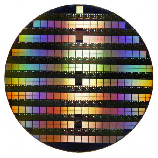
If a gas containing oxygen is used to create the plasma, it will react with the silicon on the wafer, creating silicon dioxide, an electrically conductive material. As the jet of plasma passes over the surface of the wafer in a precisely controlled manner, a layer of silicon dioxide resembling a very thin film builds up on its surface. When the etching process is complete, the silicon wafer will have a precise series of silicon dioxide tracks across it. These tracks will serve as the conductive pathways between the components of an integrated circuit.
Plasma etchers can also remove material from wafers. When creating integrated circuits, there are instances where a given device might require more surface area of the wafer to be silicon dioxide than not. In this case, it is faster and more economical to place a wafer already coated with the material into the plasma etcher and remove the unneeded silicon dioxide.
To do this, the etcher uses a fluorine-based gas to create its plasma. When the fluorine plasma comes into contact with the silicon dioxide coating the wafer, the silicon dioxide is destroyed in a chemical reaction. Once the etcher has completed its work, only the silicon dioxide pathways needed by the integrated circuit remain.
AS FEATURED ON:
AS FEATURED ON:

-
![When the plasma etching process is complete, a silicon wafer will have a precise series of silicon dioxide tracks.]() By: Vasily SmirnovWhen the plasma etching process is complete, a silicon wafer will have a precise series of silicon dioxide tracks.
By: Vasily SmirnovWhen the plasma etching process is complete, a silicon wafer will have a precise series of silicon dioxide tracks.

Discuss this Article
Post your comments