At AboutMechanics, we're committed to delivering accurate, trustworthy information. Our expert-authored content is rigorously fact-checked and sourced from credible authorities. Discover how we uphold the highest standards in providing you with reliable knowledge.
What is a Photomask?
A photomask is an opaque plate used in lithography processes. Openings or holes in the opaque surface are arranged to allow light to shine through, which transfers the pattern from the photomask onto another material, such as paper. Photomasks are commonly found in manufacturing semiconductors, where they precisely transfer images and arrangements of integrated circuits to a circuit board. This process is known as photolithography.
Photomasks play an extremely important role in the development of advanced technology in our society. Modern technology demands smaller components, which allow for devices such as very small hand-held computers and other small-scale technologies to exist. Without photmasks or lithography, the arrangements of the circuits and chips within these devices could not be transmitted accurately.
The design of a photomask is determined by chipmakers, whose exact details are described through a wide variety of languages and mediums. Due to the unique design specifications of each manufacturer, companies that produce photomasks must have a thorough understanding of the design. One of the most important parts of producing photomasks is the mask itself. In most cases, the mask is fashioned from a high-quality chrome, due to its preciseness and low fault rate.
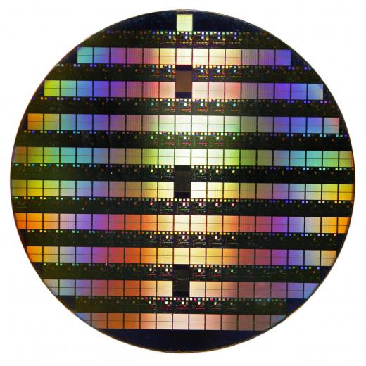
Photomasks play an essential role in the production of semiconductors, which requires lithographic procedures. Modern lithographic tools equipped with high-aperture lenses are used to transmit light through the photomask. The light projected from these devices shines through the pattern within the photomask, which is projected onto a silicon wafer. The wafer is surfaced with a photoresist, which is a light-sensitive material. A negative photoresist is then employed to remove the masked part of the material; to reverse the process, a positive photoresist is used.
Each layer of a chip requires a unique photomask. Most semiconductors have at least 30 layers, resulting in a need for at least 30 unique photomasks for every semiconductor. Photomasks, however, are far more than just a way to trace a pattern onto a chip. This is because the circuit arrangements are very precise, and their patterns must be transmitted as accurately as possible. Lithography allows for extremely accurate design transmission.
Photomasks help with the miniturization of computer chips. This is because smaller chips require highly precise images of their general arrangement, which is near impossible without a lithographic process. Without the photomask, small hand-held computers would almost be an impossibility, as their small circuits and chips require a precise arrangement.
AS FEATURED ON:
AS FEATURED ON:

-
![A silicon wafer is surfaced with a photoresist, which is a light-sensitive material.]() By: Vasily SmirnovA silicon wafer is surfaced with a photoresist, which is a light-sensitive material.
By: Vasily SmirnovA silicon wafer is surfaced with a photoresist, which is a light-sensitive material.

Discuss this Article
Post your comments