At EasyTechJunkie, we're committed to delivering accurate, trustworthy information. Our expert-authored content is rigorously fact-checked and sourced from credible authorities. Discover how we uphold the highest standards in providing you with reliable knowledge.
What Are Semiconductor Wafers?
Semiconductor wafers are 4 to 10 inches (10.16 to 25.4 cm) in diameter round disks that carry extrinsic semiconductors during manufacture. They are the temporary form of positive (P)-type semiconductors or negative (N)-type semiconductors. Silicon wafers are very common semiconductor wafers because silicon is the most popular semiconductor, owing to its abundant supply on the planet. Semiconductor wafers are a result of slicing or cutting a thin disk off an ingot, which is a rod-shaped crystal that has been doped as P-type or N-type depending on the needs. They are then scribed ready for dicing or cutting the individual dies or square-shaped subcomponents that may contain just a single semiconductor material or up to an entire circuit, such as an integrated circuit computer processor.
The semiconductor wafers used in producing electronic components such as diodes, transistors, and integrated circuits are scribed and cut to produce small dies. This suggests why the die has an X-Y formation of similar patterns that are borne by the die and actually contain up to an entire electronic circuit. Later in the production line, these dies will be mounted on a lead frame ready for bonding small wires from the die into the legs or pins of integrated circuits.
Before the semiconductor wafer is cut into subparts, there is an opportunity to test the numerous dies that it carries using automated step testers that sequentially position test probes into microscopic terminal points on the die to energize, stimulate, and read relevant test points. This is a practical approach because a defective die will not be packaged into a finished component or integrated circuit only to be rejected at final testing. Once a die is deemed defective, an ink mark blots out the die for easy visual segregation. The typical goal is that out of a million dies, less than six dies will be defective. There are other factors to consider, so the die recovery rate is optimized.
Quality systems ensure that the recovery rate for dies is acceptably high. Dies at the edges of the wafer will frequently be partially missing. The actual production of a circuit on a die takes time and resources. To slightly simplify this highly complicated production methodology, most of the dies at the edges are not further processed to save on overall cost of time and resources.
AS FEATURED ON:
AS FEATURED ON:

-
![Semiconductor wafers are pieces of silicon cut into wafers used in creating electronic components.]() By: B. WylezichSemiconductor wafers are pieces of silicon cut into wafers used in creating electronic components.
By: B. WylezichSemiconductor wafers are pieces of silicon cut into wafers used in creating electronic components. -
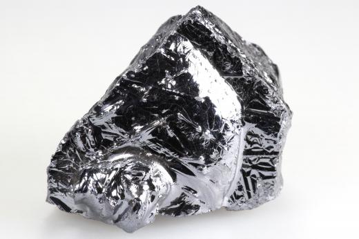
![Silicon wafers are very common semiconductor wafers.]() By: Vasily SmirnovSilicon wafers are very common semiconductor wafers.
By: Vasily SmirnovSilicon wafers are very common semiconductor wafers. -
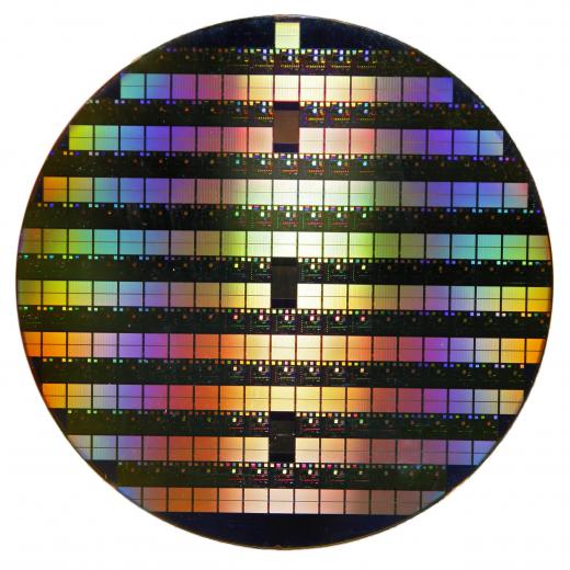
![The semiconductor wafers used in producing electronic components such as diodes, transistors, and integrated circuits are scribed and cut to produce small dies.]() By: Albert Lozano-NietoThe semiconductor wafers used in producing electronic components such as diodes, transistors, and integrated circuits are scribed and cut to produce small dies.
By: Albert Lozano-NietoThe semiconductor wafers used in producing electronic components such as diodes, transistors, and integrated circuits are scribed and cut to produce small dies. -
![Cell phones, laptops and other devices rely on silicon wafers in their integrated circuits.]() By: sepyCell phones, laptops and other devices rely on silicon wafers in their integrated circuits.
By: sepyCell phones, laptops and other devices rely on silicon wafers in their integrated circuits.


Discuss this Article
Post your comments